20+ t flip flop block diagram
Clk0 for t0-10ns 1. The four inputs are logic 1 logic 0.

9 Block Diagram For T Flip Flap Flop With Truth Table Download Scientific Diagram
Draw the block diagram of a T flip-flop using a JK.

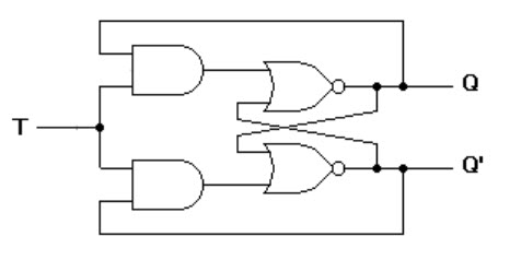
. The T flip-flop is received by relating the inputs J and K. When the clock is high and the T signal is set to low0 it will. This circuit has single input T and two outputs Qt Qt.
D flip flop is actually a slight modification of the above explained clocked SR flip-flop. The T flip flop is received by relating both inputs of a JK flip-flop. Use ModelSim to simulate the D flip-flop.
Write VHDL code behavior model to implement this positive-edge-triggered D flip-flop. The circuit diagram and truth table is given below. The S and R inputs of the RS bistable have been replaced by.
Assume the input patterns are. Draw the block diagram of a T flip-flop using a JK ff b D ff. The IC used is MC74HC73A Dual JK-type flip-flop with RESET.
It is a 14 pin package which contains 2 individual JK flip-flop inside. T Flip flop circuit diagram When the clock is set to low the output remains as it is whether the input signal is set to high or low. When T 0 both AND gates are disabled.
Flip-Flops are the basic elements of switching circuits whose main purpose is to act like an onoff switch. At different operating frequencies. The circuit diagram of the JK Flip Flop is shown in the figure below.
The operation of T flip-flop is same as that of JK flip-flop. This technique is designed through T Flip-Flop based on gated clock ALU at RTL level. Above is the pin diagram and the.
Based on the memory element switching has been classified as. Draw the block diagram of a T flip-flop using a JK. No change and Toggle.
The circuit diagram of T flip-flop is shown in the following figure. Design of Low Power Asynchronous Counter Using Reversible Logic In recent years there is a remarkable paradigm. Download scientific diagram Block diagram of T flip-flop.
Operation using11 instructions are performed in the proposed design.

Block Diagram Of The Flip Flop Circuit Download Scientific Diagram

Block Diagrams Of The Clock Generator A And The Tff As A Resettable T Download Scientific Diagram
Standard Synchronous Flip Flops A T Flip Flop B Jk Flip Flop Download Scientific Diagram

Block Diagram Of The Flip Flop Circuit Download Scientific Diagram
Sequential Circuits Basics Types Examples Its Applications

Block Diagram Of An Error Correcting Flip Flop Design Download Scientific Diagram

Block Diagram Of An Error Correcting Flip Flop Design Download Scientific Diagram

Fuzzy J K Flip Flop Neuron Block Diagram Download Scientific Diagram

Block Diagram Of The Two Processor Cpu With A Flip Flop Register Unit Download Scientific Diagram

1 Sar Block Diagram In Each Clock Cycle One Of The Outputs In The Download Scientific Diagram

Standard Synchronous Flip Flops A T Flip Flop B Jk Flip Flop Download Scientific Diagram

A Block Diagram Of A Scan Flip Flop Design B Scan Chain Download Scientific Diagram

Clocked T Flip Flop A Characteristic Table B Logic Circuits C Download Scientific Diagram

A Block Diagram Of A Scan Flip Flop Design B Scan Chain Download Scientific Diagram

Clocked T Flip Flop A Characteristic Table B Logic Circuits C Download Scientific Diagram

Block Diagrams Of The Clock Generator A And The Tff As A Resettable T Download Scientific Diagram
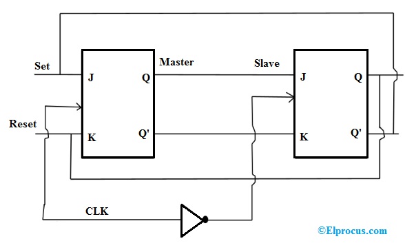
What Is A Master Slave Flip Flop Circuit Diagram And Its Working